- 您现在的位置:买卖IC网 > Sheet目录2006 > LTC2498IUHF#TRPBF (Linear Technology)IC ADC 24BIT 16CH 38-QFN
LTC2498
22
2498ff
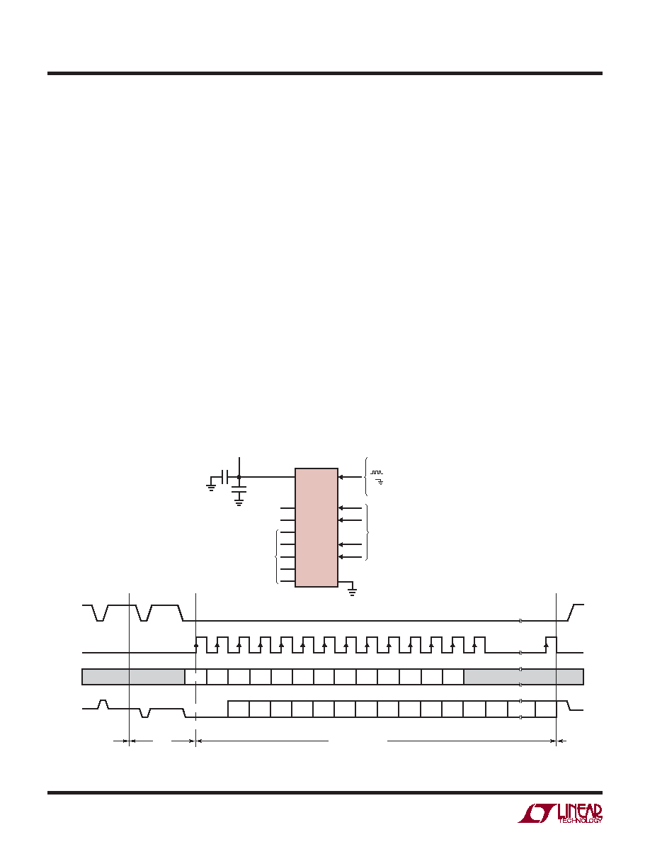
External Serial Clock, Single Cycle Operation
This timing mode uses an external serial clock to shift out
the conversion result and CS to monitor and control the
state of the conversion cycle, see Figure 6.
Theexternalserialclockmodeisselectedduringthepower-
up sequence and on each falling edge of CS. In order to
enter and remain in the external SCK mode of operation,
SCK must be driven LOW both at power-up and on each
CS falling edge. If SCK is HIGH on the falling edge of CS,
the device will switch to the internal SCK mode.
The serial data output pin (SDO) is Hi-Z as long as CS is
HIGH. At any time during the conversion cycle, CS may be
pulled LOW in order to monitor the state of the converter.
While CS is LOW, EOC is output to the SDO pin.
EOC = 1 while a conversion is in progress and EOC = 0 if
the conversion is complete and the device is in the sleep
state. Independent of CS, the device automatically enters
the sleep state once the conversion is complete; however,
in order to reduce the power, CS must be HIGH.
When the device is in the sleep state, its conversion result
is held in an internal static shift register. The device re-
mains in the sleep state until the first rising edge of SCK
is seen while CS is LOW. The input data is then shifted
in via the SDI pin on each rising edge of SCK (including
the first rising edge). The channel selection and converter
configuration mode will be used for the following conver-
sion cycle. If the input channel or converter configuration
is changed during this I/O cycle, the new settings take
effect on the conversion cycle following the data input/
output cycle. The output data is shifted out the SDO pin
on each falling edge of SCK. This enables external circuitry
to latch the output on the rising edge of SCK. EOC can be
latched on the first rising edge of SCK and the last bit of
the conversion result can be latched on the 32nd rising
edge of SCK. On the 32nd falling edge of SCK, the device
begins a new conversion and SDO goes HIGH (EOC = 1)
indicating a conversion is in progress.
At the conclusion of the data cycle, CS may remain LOW
and EOC monitored as an end-of-conversion interrupt.
applications inForMation
Figure 6. External Serial Clock, Single Cycle Operation
Hi-Z
2498 F06
Hi-Z
CS
SCK
(EXTERNAL)
SDI
SDO
CONVERSION
SLEEP
DATA INPUT/OUTPUT
CONVERSION
VCC
fO
REF+
REF–
CH0
CH7
CH8
CH15
COM
SCK
SDI
SDO
CS
GND
28
35
29
30
8
15
16
23
7
38
37
1,3,4,5,6,31,32,33,39
36
34
REFERENCE
VOLTAGE
0.1V TO VCC
ANALOG
INPUTS
= EXTERNAL OSCILLATOR
= INTERNAL OSCILLATOR
10F
0.1F
LTC2498
2.7V TO 5.5V
4-WIRE
SPI INTERFACE
EOC
BIT 28 BIT 27 BIT 26 BIT 25 BIT 24 BIT 23 BIT 22 BIT 21 BIT 20 BIT 19
BIT 29
BIT 30
BIT 31
BIT 18 BIT 17
BIT 0
1
2
3
4
5
6
7
8
9
10
11
12
13
14
32
1
0
EN
SGL
A2
A1
A0
EN2
IM
FA
FB
SPD
ODD
DON'T CARE
MSB
SIG
“0”
发布紧急采购,3分钟左右您将得到回复。
相关PDF资料
LTC2600IUFD#PBF
IC DAC OCTAL R-R 16BIT 20-QFN
LTC2602IMS8#TRPBF
IC DAC 16BIT DUAL R-R VOUT 8MSOP
LTC2604IGN-1#TRPBF
IC DAC 16BIT QUAD R-R OUT 16SSOP
LTC2605IGN-1#TRPBF
IC DAC 16BIT OCT I2C 16-SSOP
LTC2606IDD#TRPBF
IC DAC 16BIT I2C V-OUT 10-DFN
LTC2607IDE#TRPBF
IC DAC 16BIT R-R I2C 12-DFN
LTC2609CGN#PBF
IC DAC 16BIT R-R QUAD 16SSOP
LTC2621IDD-1#PBF
IC DAC 12BIT R-R 10-DFN
相关代理商/技术参数
LTC2499CUHF
制造商:Linear Technology 功能描述:ADC Single Delta-Sigma 7.5sps 24-bit Serial 38-Pin QFN EP
LTC2499CUHF#PBF
功能描述:IC ADC 24BIT DELTA SIG 38-QFN RoHS:是 类别:集成电路 (IC) >> 数据采集 - 模数转换器 系列:- 标准包装:1 系列:microPOWER™ 位数:8 采样率(每秒):1M 数据接口:串行,SPI? 转换器数目:1 功率耗散(最大):- 电压电源:模拟和数字 工作温度:-40°C ~ 125°C 安装类型:表面贴装 封装/外壳:24-VFQFN 裸露焊盘 供应商设备封装:24-VQFN 裸露焊盘(4x4) 包装:Digi-Reel® 输入数目和类型:8 个单端,单极 产品目录页面:892 (CN2011-ZH PDF) 其它名称:296-25851-6
LTC2499CUHF#TRPBF
功能描述:IC ADC 24BIT DELTA SIG 38-QFN RoHS:是 类别:集成电路 (IC) >> 数据采集 - 模数转换器 系列:- 标准包装:1,000 系列:- 位数:16 采样率(每秒):45k 数据接口:串行 转换器数目:2 功率耗散(最大):315mW 电压电源:模拟和数字 工作温度:0°C ~ 70°C 安装类型:表面贴装 封装/外壳:28-SOIC(0.295",7.50mm 宽) 供应商设备封装:28-SOIC W 包装:带卷 (TR) 输入数目和类型:2 个单端,单极
LTC2499CUHFPBF
制造商:Linear Technology 功能描述:24bit Delta Sigma ADC Temp Sens LTC2499
LTC2499IUHF#PBF
功能描述:IC ADC 24BIT DELTA SIG 38-QFN RoHS:是 类别:集成电路 (IC) >> 数据采集 - 模数转换器 系列:- 标准包装:1 系列:microPOWER™ 位数:8 采样率(每秒):1M 数据接口:串行,SPI? 转换器数目:1 功率耗散(最大):- 电压电源:模拟和数字 工作温度:-40°C ~ 125°C 安装类型:表面贴装 封装/外壳:24-VFQFN 裸露焊盘 供应商设备封装:24-VQFN 裸露焊盘(4x4) 包装:Digi-Reel® 输入数目和类型:8 个单端,单极 产品目录页面:892 (CN2011-ZH PDF) 其它名称:296-25851-6
LTC2499IUHF#TRPBF
功能描述:IC ADC 24BIT DELTA SIG 38-QFN RoHS:是 类别:集成电路 (IC) >> 数据采集 - 模数转换器 系列:- 标准包装:1,000 系列:- 位数:16 采样率(每秒):45k 数据接口:串行 转换器数目:2 功率耗散(最大):315mW 电压电源:模拟和数字 工作温度:0°C ~ 70°C 安装类型:表面贴装 封装/外壳:28-SOIC(0.295",7.50mm 宽) 供应商设备封装:28-SOIC W 包装:带卷 (TR) 输入数目和类型:2 个单端,单极
LTC2600CGN
功能描述:IC DAC OCTAL R-R 16BIT 16SSOP RoHS:否 类别:集成电路 (IC) >> 数据采集 - 数模转换器 系列:- 产品培训模块:Data Converter Fundamentals
DAC Architectures 标准包装:750 系列:- 设置时间:7µs 位数:16 数据接口:并联 转换器数目:1 电压电源:双 ± 功率耗散(最大):100mW 工作温度:0°C ~ 70°C 安装类型:表面贴装 封装/外壳:28-LCC(J 形引线) 供应商设备封装:28-PLCC(11.51x11.51) 包装:带卷 (TR) 输出数目和类型:1 电压,单极;1 电压,双极 采样率(每秒):143k
LTC2600CGN#PBF
功能描述:IC DAC OCTAL R-R 16BIT 16SSOP RoHS:是 类别:集成电路 (IC) >> 数据采集 - 数模转换器 系列:- 产品培训模块:Lead (SnPb) Finish for COTS
Obsolescence Mitigation Program 标准包装:50 系列:- 设置时间:4µs 位数:12 数据接口:串行 转换器数目:2 电压电源:单电源 功率耗散(最大):- 工作温度:-40°C ~ 85°C 安装类型:表面贴装 封装/外壳:8-TSSOP,8-MSOP(0.118",3.00mm 宽) 供应商设备封装:8-uMAX 包装:管件 输出数目和类型:2 电压,单极 采样率(每秒):* 产品目录页面:1398 (CN2011-ZH PDF)